The lithography machine has always been a hot topic in the semiconductor field. This device that can break through the process limits again and again is like a time machine, connecting the present and future of chips. Since ASML announced that it would launch the next generation lithography machine, people's attention has shifted from the latest generation of 0.33 Na lithography system to the next generation of 0.55na lithography system.
I wonder if anyone, like the author, will sigh that time is like being chased by a dog, running fast, and look forward to 2025, because according to the current news, the next generation lithography machine with a price of $400million is likely to be put into use in 2025.
So why do you need a high NA EUV lithography machine? What is the progress of the next generation lithography machine? And what challenges will it face?
Why high NA
As we all know, the main function of the lithography machine is to transfer the chip circuit diagram to the silicon chip, and the lithography technology is the key factor to determine the chip circuit size.
In chip manufacturing, the smaller the circuit, the better, because the more transistors are packaged in the same space, the higher the speed and energy efficiency of the chip. In the era of 28nm and above, the process of chip manufacturing should be relatively simple. It only needs to print the designed chip pattern on the mask and place the mask in the lithography scanner. The scanner only needs a single lithography exposure to "engrave" the circuit diagram on the chip, which belongs to the simplest single patterning process.
However, when the chip manufacturing process comes to the 22nm node, as the transistor moves from plane to 3D, the circuit diagram on the mask becomes dense, making it more difficult to "carve" the circuit diagram on the wafer, which greatly increases the difficulty and cost of the chip manufacturing process.
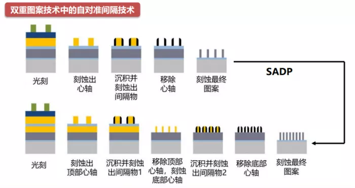
For this reason, the chip manufacturing process has shifted from the above simple single patterning process to multiple patterning. The chip circuit diagram is no longer printed on only one mask, but is divided on two or even more masks, each mask is printed separately, and finally the whole set of original drawn shapes are imaged on the wafer.
In order to print the circuit diagram on the wafer, chip manufacturers use various process schemes, such as double patterning or self-aligning schemes, which can print smaller and smaller circuits on the wafer.
Before the emergence of EUV lithography, technicians used the 193nm lithography machine, that is, the DUV lithography machine, to promote the chip technology node step by step by placing the lens in water, phase shifting mask and multiple exposure.
Founder Securities has pointed out that through self-aligning dual pattern technology and quadruple patterning process, theoretically, the DUV lithography machine can realize the 7Nm node process, but obviously, it requires an extremely large number of masks, and the process is also very complex, making mass production very difficult. At this time, EUV technology appeared.
According to Rayleigh equation, the shorter the light source wavelength used by the lithography machine, the more the semiconductor circuit with fine linewidth can be depicted. Therefore, with the extremely short wavelength of 13.5nm, EUV lithography was introduced to replace the 193nm DUV lithography machine.
For the 7 nm/6 nm nodes with a spacing of 36 nm ~ 38 nm in the chip metal layer m2 and the 5nm nodes with a spacing of 30 nm ~ 32 nm, the 13 nm resolution is enough to return the chip manufacturing process to the era of single patterning.
At present, the most advanced 5/4nm chips and 3nm chips that are expected to be mass produced this year use ASML 0.33 Na lithography system: nxe:3400c or nxe:3400d.
However, Harry Levinson of HJl graphics once pointed out that the OEM and its customers have the following options - Dual patterned EUV, triple patterned EUV or high NA when the metal layer M2 is at a spacing of 28nm or less. Now there is nxe:3400d to save 3nm. What should 2nm or even 1nm nodes do?
For the multiple patterning of EUV, experts denied it from the aspects of technology and cost.
Doug Guerrero, senior technical expert of brewer science, said: "even if we apply multiple patterning technologies to EUV, it will be very difficult to stack." Harry Levinson also pointed out that from an economic point of view, it is meaningless to think of dual mode.
Thus, in order to continue Moore's law, the optimal solution is high NA. Na is the numerical aperture of the optical system, which represents the incident angle of light. A larger Na lens can print a smaller structure. For example, 0.55 Na can achieve 8nm resolution.
On the one hand, high NA EUV can reduce the cycle time of the wafer factory, because the total processing capacity required for a single high Na is less than the total processing time for multiple passes of 0.33 Na EUV.
On the other hand, it also improves the flexibility of chip design. Some design elements can only be realized in a single mask, and high NA provides an improved imaging window for these elements. More importantly, the reduction of process steps can also improve the output of chips. In this respect, high NA EUV is the inevitable choice.
How is it going now
Now that the schedule of ASML's next generation EUV 0.55 Na lithography machine has been worked out, what is its progress now?
According to the latest news, ASML executives at its headquarters in Veldhoven, the Netherlands, told Reuters that the prototype is expected to be completed in the first half of 2023. In other words, the prototype will be completed in a year.
In addition, ASML CEO Peter wennink disclosed in April that the first high NA system has been integrated in the new clean room in Veldhoven. In the first quarter of this year, we received several orders for the exe:5200 system, and we also received additional orders for the exe:5200 system in April. At present, ASML has received high NA orders from three logic vendors and two storage vendors.
At the same time, ASML is also establishing a test laboratory with the Belgian Electronic Research Center IMEC, in which a high NA system will be built, connected to the coating and development track, equipped with measurement equipment, and the infrastructure accompanying the development of high NA tools - including deformation imaging, new mask technology, measurement, resist screening and film patterned material development, and is preparing to use the production model as early as 2025, Achieve mass production in 2026.
Of course, as a "colossal giant" composed of multiple modules and hundreds of thousands of parts from nearly 800 suppliers around the world, the efforts of ASML alone are not enough. Other manufacturers related to lithography have also gone to the battlefield.
In terms of lens, Zeiss and ASML will use a deformable lens on the high NA lithography machine. They maintain a 4 × Lens reduction solves the problem that the maximum exposure field size on the wafer is too small, resulting in 26 mm × 16.5 mm field size for high NA EUV lithography.
In addition, the narrow incidence angle range of multilayer mirrors with high reflectivity has an impact on the lens and mask. Extending the lens design concept of the current generation of 0.33 Na lens to 0.55 Na will lead to a large incidence angle of the mirror, which is problematic.
Therefore, Zeiss uses a different type of high numerical aperture design to reduce the maximum incident angle on the reflector. A basic feature of this new design is central shadowing. High performance lenses with central shadowing have been used in other applications, such as astronomy. The Hubble Space Telescope is a well-known example.
For high naeuv, Japanese test equipment manufacturer lasertec is developing a new photochemical blank detection (ABI) system for EUV mask blank with 1nm x 30nm sensitivity. Masashi Sunako, President of USA, once said that "our goal is to locate defects with an accuracy of 10nm."
It is understood that lasertec has also introduced a photochemical pattern mask detection (APMI) system using a 13.5nm light source, which can locate 20nm defects on the EUV mask. Of course, its APMI system for high NA EUV mask is also under development. It is reported that the design of new optical devices, detectors and systems has been completed and is planned to be used in 2023/2024.
In addition, KLA and nuflare are also developing a multi beam electron beam mask detection tool. Nuflare is developing a multi beam detection system with 100 beams, which is planned to be launched in 2023. Tadayuki sugimori of nuflare pointed out that the sensitivity of the system is 15nm, and the inspection time of each mask inspection cycle is 6 hours.
In the future, there are still many challenges
Even though the manufacturers are working hard, it is still a big challenge to manufacture high NA EUV.
Recently, the paper "high numerical aperture EUV lithography: current situation and future prospects" published in the Japanese Journal of Applied Physics in April listed eight challenges faced by high NA EUV, which are: failure to meet the resolution requirements, random phenomena and pattern collapse may affect the yield; Light source that can support photon shot noise and productivity requirements; Solution meeting 0.55 Na small focal depth; Polarization control for maintaining high contrast at 0.55 Na; Calculate lithography capability; Mask manufacturing and metering infrastructure; Large chip solutions; High NA EUV lithography cost.
· resolution requirements
For a long time, photoresist has restricted the lithography ability of EUV, and with the development of technology, it has been thinning, which also makes the line edge roughness (LER) increase. As early as ARF lithography, people had realized the problem of LER, but it had little impact on chip manufacturing at that time. However, with the continuous miniaturization of process nodes, ler began to affect linewidth control and device performance.
To reduce the impact of LER, we must achieve low LER.
On the other hand, many different types of EUV photoresists have a common feature, that is, blur. In addition to the image blur caused by electrons, during baking after exposure, the chemical amplification resist will also have additional blur due to the diffusion of photo acid, which will also affect the yield to some extent.
Current, at 10 nm ½ The research and development of photoresists with the target of spacing and below is still in progress, and many problems existing in chemical amplified photoresists must be overcome. However, photoresists with low ler, low-level randomness defects, no pattern collapse and necessary resolution, and avoiding excessive exposure dose have not been found yet, so they need to be further developed and improved.
· light source
Whether it is photoresist or other specific material formulations, there is a dose below which the ler and defects caused by photon shot noise are too large to meet the technical requirements. Therefore, a light source with high enough output power is required to avoid reducing throughput and productivity.
The throughput of ASML's EUV exposure tool is a function of the source power (W) divided by the exposure dose (MJ cm -2). The arrow indicates the point of the tool with a 500 W source and an exposure dose of 80 MJ cm -2.
ASML sandiego uses its laser generated plasma (LPP) light source to achieve 400-500 W output. By converting infrared laser into EUV light in the band, it improves the repeatability between pulses and increases the output of LPP light source. In addition, free electron laser is considered as a substitute for LPP light source. At present, ASML is still trying to achieve higher optical output.
· solution meeting 0.55 Na small focal depth
Depth of focus (DOF) has always been a challenge for optical projection lithography. When Na is 0.55, DOF decreases significantly, about 1/3 of 0.33 Na. Therefore, it is necessary to improve the focusing control to achieve high numerical aperture EUV lithography.
In this regard, in order to obtain good imaging, photoresist thinning is very important. However, when the photoresist film becomes very thin, there will be phenomena such as component segregation, reducing patterning.
In addition, focus control is not only a problem in lithography, but also puts forward higher requirements for wafer flatness, which also puts forward strict requirements for thin film deposition, especially chemical mechanical polishing (CMP).
· polarization control for maintaining high contrast at 0.55 Na
In high Na, the image contrast depends on the polarization of the illumination. As shown in the figure below, the image contrast of the two interference plane waves can be maintained under the large NA of s-polarized light, but with the increase of Na, the contrast of p-polarized and non polarized light becomes smaller. For this reason, the illumination system of the immersion lithography machine provides polarization control, and the laser generated plasma (LPP) light source initially used on the high NA exposure tool is planned to generate non polarized light.
When using non polarized light at 0.55 Na, the image contrast will decrease significantly. On the other hand, the emission of the free electron laser is polarized, which provides additional power for considering the free electron laser (FEL) as the light source of the high NA EUV exposure system.
Image comparison of two interference plane waves supported by a given numerical aperture at the maximum incident angle.
For s-polarization, the polarization vectors are perpendicular to the incident plane, while for p-polarized light, they are located in the incident plane.
· calculate lithography capability
Many physical phenomena need to be considered in the calculation accuracy, and the small focal depth associated with high NA increases the demand for calculation solutions. At present, reverse lithography (ILT) has been proved to be able to construct mask layout that maximizes the process window, and the optimal mask layout resulting from the application of ILT usually presents a curve, making mask manufacturing more difficult.
The multi beam mask writer solves this problem, which not only makes it possible to produce high-quality masks with curve patterns, but also starts to standardize the data format of curve features on the mask. Although ILT and curve features are not unique to high NA EUV, these functions are gradually mature on high NA EUV, so they are expected to become an important part of high NA technology.
· mask manufacturing and metering infrastructure
Photomask is an important part of chip manufacturing. As the circuit diagram becomes smaller and smaller, the deviation from the ideal mask becomes larger and larger, which affects the final wafer pattern. Therefore, it is necessary to solve the mask problems, including reducing the 3D effect of the mask and enhancing the service life of the mask.
Most importantly, the introduction of new photomask types into the high NA EUV optical system also brings additional complexity to the mask industry.
The current tantalum based absorbers are usually about 60-70nm thick, designed to absorb a sufficient amount of light. Compared with the 13.5nm wavelength, the thickness is larger. Therefore, irradiating the mask at a specific incident angle (centered at 6 ° in traditional EUV lithography) will distort the aerial image, eventually transfer to the light pattern in the photoresist, and reduce its image contrast.
These so-called mask 3D effects are also accompanied by more feature related changes and the best focus on the wafer, which poses an additional challenge to the high NA EUV lithography technology with reduced DOF.
Of course, as the mask becomes more and more complex, the requirements for equipment are also increasing.
· large chip solutions
At present, large chips are very popular, but they are too large to adapt to the needs of high NA exposure tools ½ Field. In order to continue to produce chips with similar sizes, splicing is required. In other words, some chips use one mask for pattern transfer, while the rest are exposed by the second mask for pattern transfer.
Splicing is not a new lithography technology, but it needs to be implemented very accurately. In addition, since EUV absorbers cannot completely and effectively suppress reflected light, multilayer reflectors around the exposed area of the mask are often removed by etching, and etching the black frame will reduce local stress, thereby affecting the mask features.
· cost of high NA EUV lithography
Cost has always been a concern of the lithography machine. The price of the lithography machine is not expensive for two days. Obviously, the high NA EUV lithography machine will only be more expensive, and its cost is expected to exceed US $300million. For previous generations of lithography machines, the exponential increase in price is offset by the increase in throughput, which shows that the throughput of lithography machines is particularly important.
Therefore, how to improve the throughput of the lithography machine has become the key. From this point of view, improving the power of the light source is one of the solutions. On the one hand, ASML San Diego has achieved 400-500 w source power for LPP sources, and plans to achieve higher power.
On the other hand, in addition to providing polarized light, the free electron laser is expected to have high power, which is another reason for considering the free electron laser as the light source of EUV lithography.
However, when the light source is higher than 800 W, the throughput ofhigh Na EUV lithography machine will approach the mechanical limit, and then it will face new problems
Write at the end
In general, it has become the only way for the lithography machine to move towards high Na to "extend the life" of Moore's law. At the SPIE advanced literature and pattern held a few days ago, it even began to discuss how to turn to 0.7 Na EUV. However, it is clear that there are still many challenges ahead of us.