A new type of semiconductor material called "two-dimensional semiconductor" has recently made breakthroughs in research and development. In the future, it may not only replace silicon as a semiconductor raw material, but also become a magic weapon of Moore's law. The Korean Academy of science and Technology (Kist) recently announced that through the development of a new ultra-thin electrode material, it has successfully enabled electronic and logic devices based on two-dimensional semiconductors to freely control their electrical performance.
In addition, research teams from Nanyang University of technology, Peking University, Nanjing University and other universities have also made breakthroughs in two-dimensional semiconductor integration and material growth.
At the same time, domestic listed companies are also accumulating strength to develop and reserve relevant technologies, which may benefit from this cutting-edge technology in the future.
Chinese and foreign scientific research teams have made breakthroughs in succession
In 1965, Intel co-founder gordonmoore put forward the famous Moore's Law: the number of components that can be accommodated on an integrated circuit will double every 18 to 24 months, and the performance will also double. This means that the physical size of transistors on a silicon chip per unit area is getting smaller and smaller, and the number is increasing. But today, a chip the size of a fingernail can carry 10billion transistors, and silicon transistors are reaching their physical limits. The continuation of Moore's law requires completely different new materials and equipment.
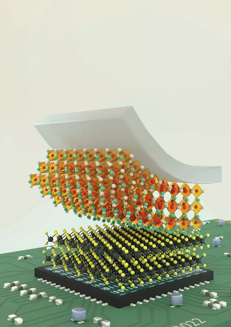
In recent years, two-dimensional semiconductor, which is widely expected, is one of them. Because traditional silicon transistors are based on three-dimensional bulk semiconductors, it is difficult for electrons to pass through nanoscale channels. However, the two-dimensional material can further reduce the size of the transistor, making it an ultra-thin crystal chip at the atomic level, which facilitates the relatively free flow of charges.
The Korean Academy of science and Technology (Kist) recently announced that the joint research team led by Dr. do Kyung Hwang of the optoelectronic materials and devices center and Professor kimoon Lee of the Department of physics has successfully enabled the electronic and logic devices based on two-dimensional semiconductors to freely control their electrical properties by developing a new ultra-thin electrode material (cl-snse2).

Source: Wiley online library
This research solves the problem that it is difficult for traditional two-dimensional semiconductor devices to realize complementary logic circuits (only showing the characteristics of n-type or p-type devices) under the Fermi level pinning phenomenon. Using the new electrode material, a single device can perform the functions of n-type and p-type devices at the same time, and a high-performance, low-power, complementary logic circuit can be obtained, which can perform different logic operations.
Dr. do Kyung Hwang predicted that the developed two-dimensional electrode material is very thin, showing high light transmittance and flexibility. Therefore, they can be used in the next generation of flexible transparent semiconductor devices.
Researchers from Nanyang University of technology, Peking University, Tsinghua University and Beijing Institute of quantum information science recently demonstrated the successful integration of single crystal titrated strontium (a high-k perovskite oxide) with two-dimensional semiconductors using van der Waals. This method can open up new possibilities for the development of new transistors and electronic components.
Team approach schematic image source: Tech Xplore
Single crystal titration of strontium is a perovskite oxide. It has been found that it is almost impossible to combine perovskite oxide with materials with different atomic structures. However, the intelligent method adopted by the team successfully bypasses this limitation and can achieve almost unlimited material combinations.
The researchers said that the transistors they created can be used to manufacture high-performance and low-power complementary metal oxide semiconductor inverter circuits. In the future, their devices can be manufactured on a large scale to develop low-power logic circuits and microchips.
Not long ago, the team of Professor wangxinran of Nanjing University and Professor wangjinlan of Southeast University announced that the epitaxial growth of double-layer molybdenum disulfide (one of the known two-dimensional semiconductor materials with the best photoelectric performance) film with large area and uniform thickness was realized for the first time in the world.
"This research has not only broken through the bottleneck of the layer number controllable epitaxy growth technology of large-area uniform double-layer molybdenum disulfide and developed the highest performance molybdenum disulfide transistor devices, but also the new mechanism of layer number controllable nucleation of double-layer molybdenum disulfide is expected to be further extended to the epitaxial growth of other two-dimensional material systems, providing a new direction and choice for the alternative materials of post silicon-based semiconductor electronic devices." Ma Liang, co-author of the paper and professor of Southeast University, said.
In the known studies of molybdenum disulfide, double-layer molybdenum disulfide has higher carrier mobility and larger driving current than single-layer molybdenum disulfide, and has more advantages in the application of electronic devices. However, the double-layer molybdenum disulfide obtained by the traditional growth mode has the problems of poor uniformity of layers and film discontinuity. The team made a breakthrough in the substrate induced double-layer nucleation and the new growth mechanism of "going hand in hand".
Competition between Intel and TSMC domestic listed companies are also making efforts
In addition to the scientific research team, the business giants are also vigorously promoting their research and development in the field of two-dimensional semiconductors. Who can achieve transistor miniaturization one step ahead of his competitors will have the say in the future chips and even in the field of science and technology. This competition may even determine who will be the chip overlord in the next decade.
At the IEEE International Electronic equipment conference held last December, Intel and TSMC demonstrated their solutions to the problem of high resistance and low current of two-dimensional semiconductors. There is a sharp resistance point at the place where the semiconductor contacts with the metal, which is the biggest obstacle of two-dimensional semiconductor at present. TSMC and Intel use semi metallic antimony as contact material to reduce the energy barrier between semiconductors and contacts, so as to realize the low resistance connection between two-dimensional semiconductors and devices.
TSMC has been looking for two-dimensional materials that can replace silicon since 2019. Last May, TSMC took the lead in announcing the discovery that semi metallic bismuth can be used as a bonding material for two-dimensional semiconductors to achieve extremely low resistance. However, bismuth has the defect that the melting point is too low to withstand the high-temperature processing of subsequent chips.
It is worth mentioning that the R & D of two-dimensional semiconductor is not only the battlefield of giants, but also the presence of domestic listed companies.
In September, 2021, the research group of Professor wangxinran from the school of Electronic Science and engineering of Nanjing University broke through the key technologies of two-dimensional semiconductor single crystal preparation and heterogeneous integration, including the cooperation of Tianma Microelectronics Co., Ltd. (Shenzhen Tianma a). This breakthrough provides a new technical route for the future development of micro LED display technology. At that time, some investors immediately asked shentianma a. the company replied and confirmed that the above breakthrough news was true, and the company participated in relevant research.
At present, the two most studied two-dimensional semiconductor materials, molybdenum disulfide and tungsten disulfide, are also involved by companies.
Jinmo Co., Ltd., a professional molybdenum producer, successfully applied graphene like molybdenum disulfide to lithium-ion batteries in August last year. In terms of two-dimensional semiconductor applications, the company told reporters that molybdenum disulfide, as a cutting-edge material, has been produced and sold on a small scale, but it currently accounts for a very small proportion of the company's products, and the application situation is not clear.
In June, 2021, del, a company in the field of home furnishings and new materials, disclosed on the investor interaction platform that the company's holding subsidiary, graphene, has technical reserves of molybdenum disulfide preparation equipment, which is mainly used to prepare molybdenum disulfide two-dimensional semiconductor materials.
However, del future insiders told reporters that the company's technical reserves have not been further promoted and there is no commercial production. The technology reserve is related to the company's strategy, and the specific application is still uncertain.