Moore's law proposed by Intel founder Gordon Moore is the golden rule of the semiconductor industry. It has guided the industry forward for more than 50 years and upgraded the next-generation process in two years. However, the saying that Moore's law is dead has also been spread for many years, because it is more and more difficult to iterate the chip process after the 28nm node. Although Intel, Samsung, TSMC and other companies rely on various technical means and marketing publicity to push the CPU logic process all the way to the 5nm node, and will enter the 3nm node next year, they will still face greater challenges in the future.
Especially after 1 nm, the quantum tunneling effect may invalidate the semiconductor.
How will the future technology go? At the recent future summaries 2022 conference, IMEC (Belgium Microelectronics Center) showed the latest roadmap and saw the 0.2nm process in 2036
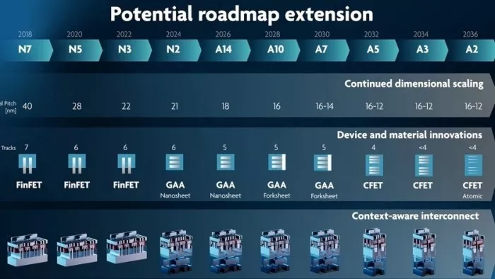
In short, after the trial production of N3 process this year, there will be 2nm process in 2024 and A14 process in 2026 - A represents Amy, which is the scale after nano. A14 process can be understood as 1.4nm process. A20 and A18 processes proposed by Intel are equivalent to 2nm and 1.8nm processes.
We also reported a few days ago that TSMC will turn its team to the future 1.4nm process research and development after the completion of the research and development of the 3nm process, which is expected to start in June.
Then look at the road map. IMEC expects to realize A10 process, that is, 1nm node in 2028, A7 process in 2030, followed by A5, A3 and A2 processes respectively. A2 in 2036 is about equivalent to 0.2nm node**
The roadmap of IMEC is basically developed according to Moore's law, which proves that the chip process can be iterated in the future.
However, it should also be noted that the pole distance index of MP metal gate that really determines the process density does not change as much as the process number. Even A7 to A2 processes are between 16-12nm, and the density may not be improved**
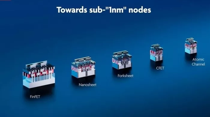
At the same time, to realize the process of 1nm and below, the transistor architecture also needs to be changed. We know that TSMC and Samsung will give up FinFET and turn to GAA structure at 3nm or 2nm node, and turn to CFET transistor structure after A5.
There are many other technological upgrades, including wiring, lithography and so on, which require a series of technological breakthroughs.
In short, the challenge is huge. You know, IMEC's prediction is still very optimistic, but in the development of the next 10 years, it is impossible for the new process not to skip the ticket, and the 0.2nm process may not be possible until 2040.