In the past two years, if you want to change Android partners, you must have heard such a roast: "888, 8gen1, X do not buy!" Although this is a joke, we can also see how "cool" Android's flagship products have been to us in the past two years. The "best performance" at the press conference can be heard every year, but the power consumption can't stop.

Let's move forward three years.
At that time, who had nothing to do with how many good heat dissipation black technologies they used..
But there's no way. Everyone scolds. There's no other choice if you want to change an Android machine.
But I can't help asking.
Why is Qualcomm so hot these two years

Fever is inevitable
We know that as long as we do work, it will bring fever.
For the chip, the heating is mainly composed of dynamic power consumption and static power consumption.
*Dynamic power * mainly refers to the heat generated by the chip during operation, including the charge and discharge of the circuit and the jump of the working state of the transistor.
**Static power mainly refers to various types of leakage current and competitive current in the chip.
Taking the switch as an example, dynamic power consumption is like the power consumption generated by repeatedly switching the switch.

The static power consumption is like the power consumption generated by the switch standing in place in order to maintain its current state (on or off).
The chip we made...
Naturally, it is hoped that the transistor density will be higher and higher, the performance of the corresponding chip will be stronger and stronger, and the power consumption will be lower and lower
However, the chip doesn't talk about "ideal" with you.
In recent years, we have made the "switch" smaller and smaller, and the dynamic power consumption has indeed been reduced a lot.
However, with the development of nano chip design, the problem of power leakage becomes more and more serious.
The reason can be understood as that the "switch" is too thin to stop the electronic "smuggling" on both sides...
So if you want to reduce this leakage, you need a whole new structure and new materials.
Rebuild the switch that is thin and can block "smuggling".
When the chip reaches 28nm, this technology is FinFET (fin field effect transistor).
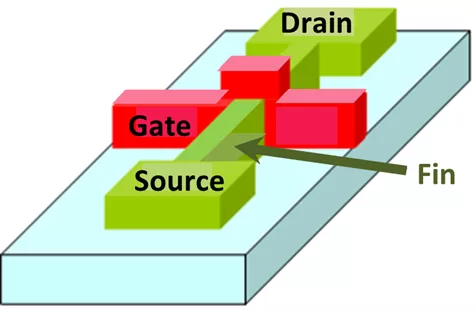
Now the process is slowly reaching 5nm, and FinFET is not very effective.
The leakage level is like a circle, which returns to the dilemma of the 28nm process in that year.
At this time, the big guy poured out a new future process to solve the problem, which is called GAA (all ring gate transistor).
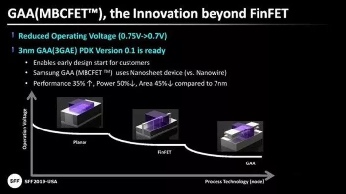
The difference between these two processes is simply to expand from two-dimensional to three-dimensional.
The contact range is increased and the leakage can be better controlled
However, for reasons of conservatism and process validation, no one has used GAA yet.
Therefore, we have no choice at present. We can only continue to use the old process FinFET for 5nm.
The electric leakage problem is hard resisted by sewing and mending

Is it craft
Since everyone is hard to resist this leakage, why can the apple next door control the energy consumption so well?
I have to mention the well-known first pot bearer:

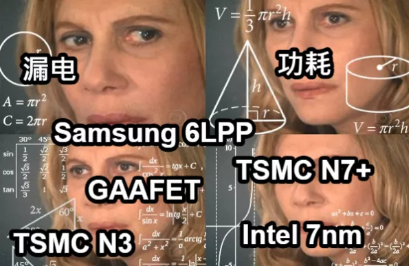
Unlike apple, Qualcomm's SOC of these two generations are manufactured by Samsung.
Despite Samsung and TSMC, they call their technology 5nm.
However, in today's FinFET era, the name of the process does not correspond directly to the physical parameters of the chip, which is more like the name of a technology node.
The transistor density gap made by the two 5nm processes can even plug in the 14 nm of Intel. In terms of transistor density alone, TSMC's 5nm process can place 17.13 million transistors per cubic millimeter, or 171.3 MTR.
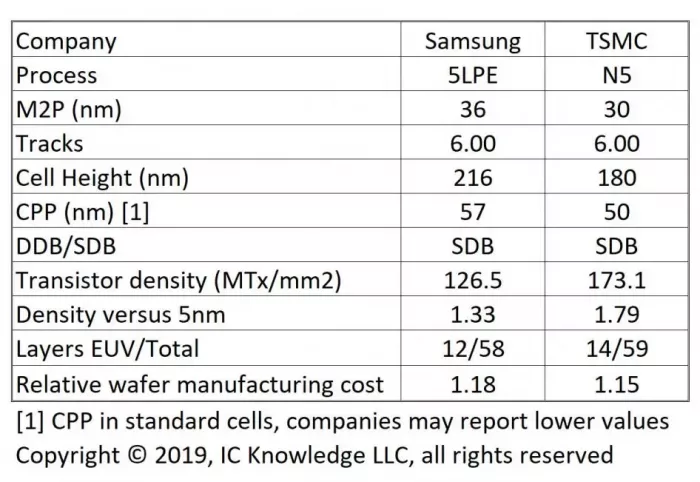
Samsung's 5nm can only achieve the level of 126.5mtr.
Here I would like to mention a little additional knowledge. The reason for these differences in transistor density is related to the technical iteration route of the two manufacturers.

Let's make a long story short. For TSMC, we can understand it as TSMC's 7Nm - & gt; 5nm is a complete technical iteration route.
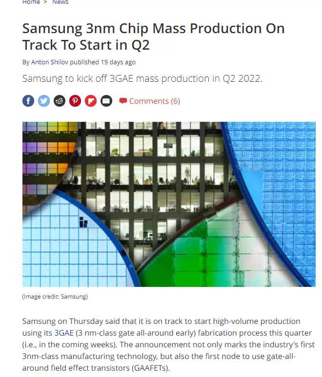
On the other side of their plan, many Samsung - & gt; 3nm is a complete technical iteration. They intend to launch a new GAA directly on the 3nm process.
Therefore, for Samsung, its 5nm process is slightly conservative compared with its own 7Nm progress.
But to be honest, from the perspective of a single transistor, this gap is actually good.
Others believe that the yield of Samsung technology is also worth saying
Two months ago, a news showed Tony a smile
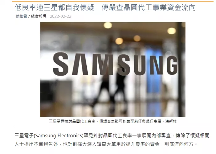
No, why is your yield low? You don't count it in your heart
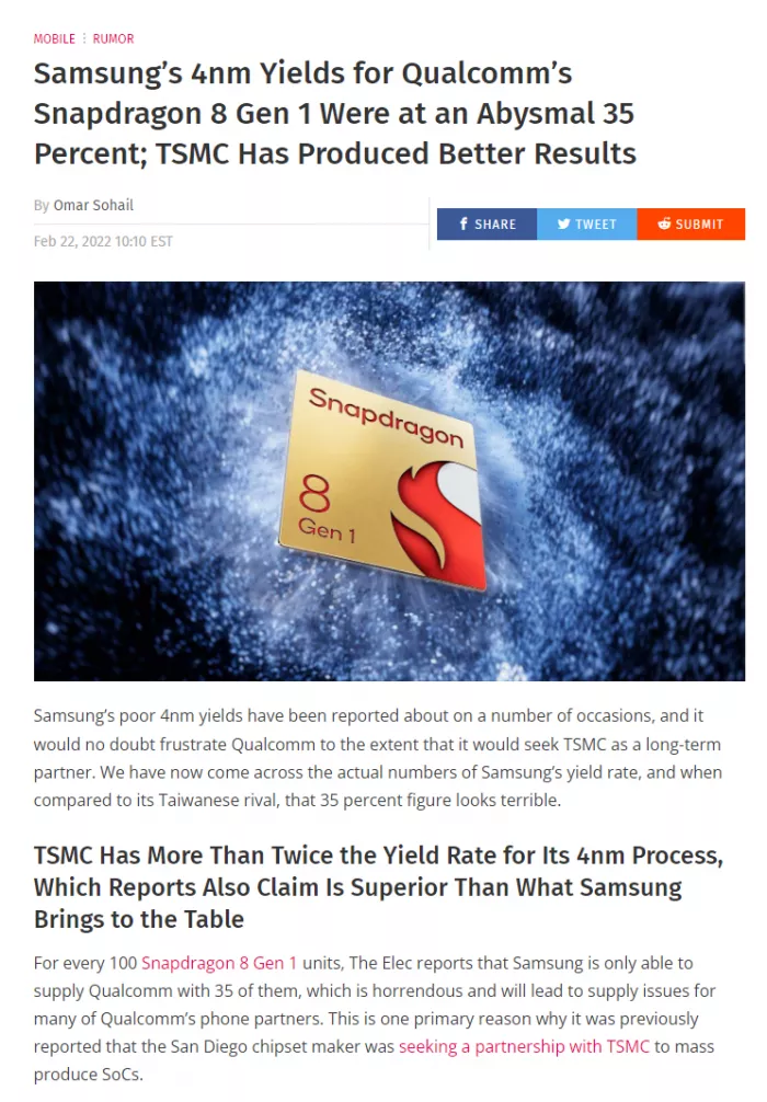
According to @ wccftech, the yield of Samsung's Wafer Foundry Department in the 4nm process is only 35%.
The yield rate of Samsung 3nm GAA technology, which is still under development, is only 10% ~ 20%.
According to DIGITIMES, Samsung has lied about the yield rate in 5nm, 4nm and 3nm processes.
We don't even know whether the yield is before or after the false report.
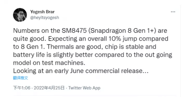
I don't know if this is the reason. Qualcomm decided to hand over the 4nm 8 GEN1 plus to TSMC for OEM.
Oh, by the way, what is the yield rate of TSMC's 4nm process next door?
70% 。。 Of course, when we analyze the gap between process and density here, we can only say that we are making a side talk about the gap between Samsung and TSMC.
But in Tony's view, the hot "black pot" can not be lost to the OEM of Samsung.
Or is the architecture untenable
Why does Tony think it's wrong to blame Samsung?
Because Tianji 9000 is here.
The power consumption of the Tianji 9000, which we once placed high hopes on and handed over to TSMC, is not very ideal.
Data source, geek Bay ▼
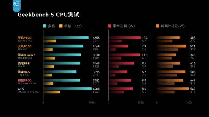
In some test scenarios, you can't even beat your little brother Tianji 8100.
So... Will the problem lie in the arm public architecture they adopt?
Tony, let's analyze. The architectures of Xiaolong 8gen1 and Tianji 9000 SOCS are very consistent, using the 1 + 3 + 4 structure of arm public version.
That is, 1 x2 super nucleus + 3 a710 large nuclei + 4 A510 small nuclei.
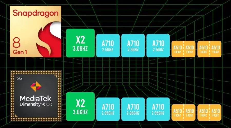
Just look at the performance at the press conference, but what is the level of these nuclear heating?
It can only be said to be terrible.
Under the test of geekbench 5, the power consumption of large core a710 can reach 2.1W, while the single core power consumption of super large core x2 can even exceed 4W
A single core!
You know, under the test, the whole CPU of Xiaolong 865, the generation of God u, can only reach 6.7w...
Although the running performance of 8gen1 and Tianji 9000 has gone up, the nearly doubled heat is not something that ordinary mobile phones can carry.
In the past two years, Tony knows that the mobile phone that can suppress the heat dissipation looks like this:

Yes, you have to plug the fan in.
According to the tests of other media, when 8gen1 is fully powered, the peak power consumption of CPU and GPU can both exceed 10W!
Apple next door also has a chip that can break through 10W in the past two years. Poor friends may wish to guess what it is?

It is M1 of mobile terminal.
With the same 10W power consumption, what can you do with M1... What can this 8gen1 do...
God is making 8gen1 ▼

And there is another case. Now arm is optimized for 64 bit applications. Under high load, it can use super core X2, and under low load, it has prepared small core A510.
Therefore, when arm runs 64 bit applications, it should have performance and power consumption
However, since the Android camp has not eradicated 32-bit applications, arm only retains the large core a710 to run 32-bit programs.
Therefore, once Android phones run 32-bit applications, regardless of the application load, they have to be thrown onto the big core a710. Even if this application is a notepad, a710 has to run.
This result... No wonder it's not hot.
Apple is different. It has studied its own architecture since A7, and has been updated to A15 this year.
And the public version of arm is not mixed at all
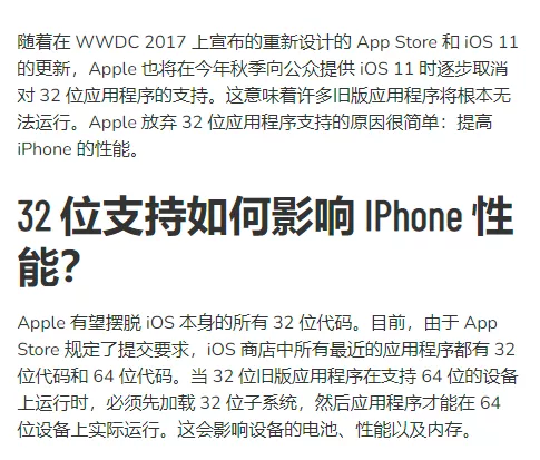
Moreover, apple is also a ruthless role, throwing away the burden of 32-bit applications in 2017.
So it seems that Apple's overall power consumption is better controlled.
It's hot, and then
We can understand why the high-end chips on Android are so hot.
Process technology with increasingly serious leakage + Samsung's 5nm "water injection" + arm's public version architecture design is too radical + arm has made sacrifices to be compatible with 32-bit applications.
These sets of Wolong chicks are just coming together
The final result is that consumers are dumb to eat Coptis chinensis. The mobile phone is really not hot...

Fortunately, manufacturers are not people who are blind and don't know how to change.
After all, on the way of exploring new technology, who can say that he will never overturn?
TSMC was jokingly called "Taiwan leakage" because of process problems at 28nm.
Samsung's bet is naturally the planned 3nm process GAA. According to industry news, GAA can even pull the process to the equivalent 1nm.
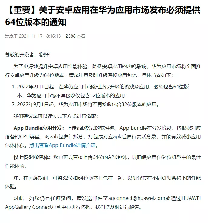
For mobile phone manufacturers, the "exclusion" of 32-bit applications is becoming more and more obvious. Moving faster and faster.
This year, when many mobile phone built-in app stores put on the shelves, they also began to force developers to upload 32-bit and 64 bit applications at the same time. Everyone uses 64 as applications, and the phenomenon of big core waste will disappear.
Now, Qualcomm has acquired nuvia, a startup founded by Gerard Williams, a former chief architect of apple, for $1.4 billion.
Although there is still some distance to re-establish their own architecture self-research team.
However, they also hope to reduce their dependence on ARM architecture with the help of their team's R & D experience. One day, it is not impossible for Qualcomm's own chips to catch up with apple.

Incidentally, the next few days will be Qualcomm's new product launch.

The products brought by then, even if they are not the 8 GEN1 plus we are thinking about, are mostly new chips manufactured by TSMC.
Although we are generally not optimistic about the architecture of arm this time.
But I'm not sure. Will TSMC's extraordinary performance this time bring us a surprise?
Picture and data source:
Some pictures come from the Internet
Part of the data comes from geek Bay
Why is Samsung 4nm inferior to TSMC 4nm?
The road of training for Digital IC back-end design engineers Yan futi
https://www.qualcomm.com/news/releases/2021/01/13/qualcomm-acquire-nuvia
https://zh.wikipedia.org/zh-mo/FinFET
https://m.eprice.com.tw/mobile/talk/102/5717005/1/
In depth analysis | why did the 5nm chip overturn collectively? The problem that plagued TSMC Samsung 10 years ago is back - xinhehui