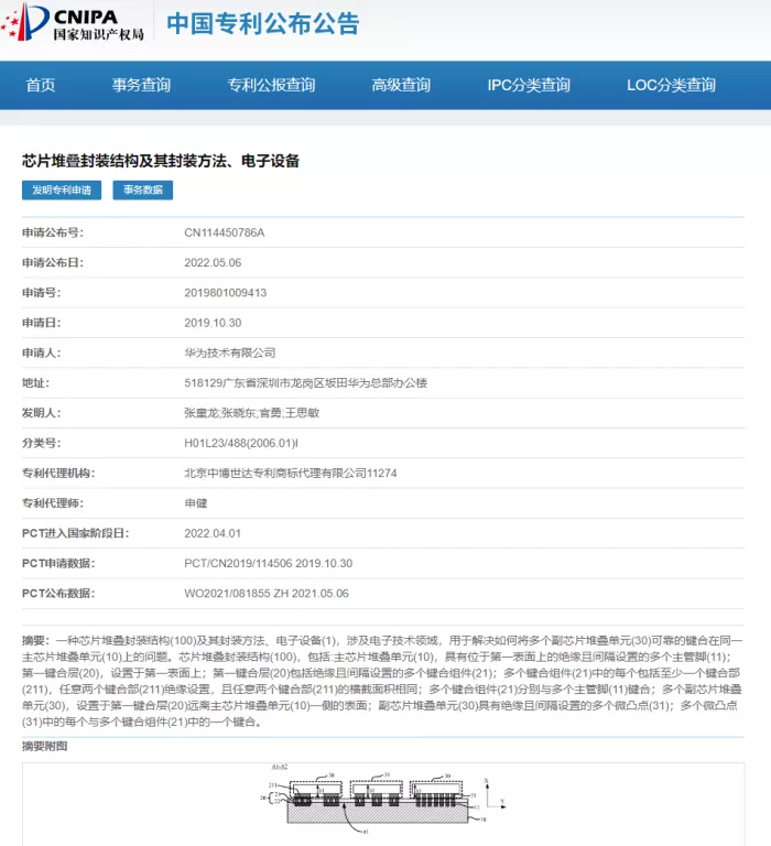
According to the State Intellectual Property Office, on May 6, Huawei announced a patent on "chip stacking packaging structure, packaging method and electronic equipment", and further disclosed Huawei's stacking chip technology. The application publication number is cn114450786a* This patent was applied for * as early as October 30, 2019. The inventors are Zhang tonglong, Zhang Xiaodong, Guan Yong and Wang Simin.
The patent describes a chip stacking packaging structure, its packaging method and electronic equipment, which relates to the field of electronic technology and is used to solve the problem of how to reliably bond multiple sub chip stacking units to the same main chip stacking unit
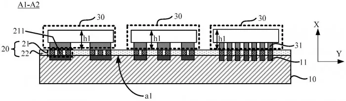
The chip stack package structure includes:
- A main chip stacking unit (10) having a plurality of insulated and spaced main pins (11) located on the first surface;
- A first bonding layer (20) arranged on the first surface; The first bonding layer (20) comprises a plurality of bonding components (21) insulated and arranged at intervals;
- Each of the plurality of bonding assemblies (21) includes at least one bonding part (211), any two bonding parts (211) are insulated, and the cross-sectional areas of any two bonding parts (211) are the same;
- A plurality of bonding components (21) are respectively bonded with a plurality of main legs (11);
- A plurality of sub chip stacking units (30) arranged on the surface of the first bonding layer (20) away from the main chip stacking unit (10);
- The sub chip stacking unit (30) has a plurality of insulated and spaced micro bumps (31);
- Each of the plurality of micro bumps (31) is bonded with one of the plurality of bonding assemblies (21).
In early April, Huawei also disclosed a patent for chip stack packaging and terminal equipment, application Publication No.: cn114287057a, involving the field of semiconductor technology, which can solve the problem of high cost caused by the adoption of silicon through-hole technology while ensuring the power supply demand
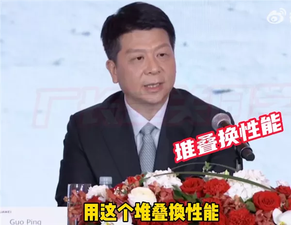
At the press conference of Huawei's 2021 annual report at the end of March, Huawei's rotating chairman Guo Ping said, in the future, Huawei may adopt the chip design scheme of multi-core structure to improve the chip performance. At the same time, it adopts the methods of area for performance and stack for performance, so that the less advanced technology can continue to make Huawei competitive in future products**