AMD CPU + GPU is being fully integrated. The next generation of Ruilong 7000 series processors will integrate zen4 and rdna2 architectures. In the field of high-performance and high-performance computing, insict accelerator card will do the same. Amd has released the insict mi200 series accelerator card. Based on cdna2 architecture, it adopts MCM dual core packaging for the first time. The next generation of insict mi300 has also been exposed before, and may adopt crazy four core packaging.
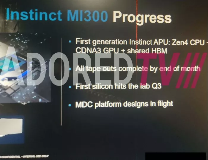
A spy photo exposed by adoredtv shows that mi300 is called "the first generation insight APU", which will integrate zen4 CPU architecture, rdna3 GPU architecture and HBM high bandwidth memory at the same time**
The progress of mi300 is quite rapid, all the wafers will be completed by the end of this month and the first silicon wafer will be obtained in the third quarter**
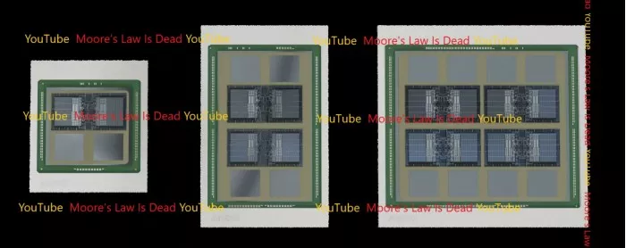
Interestingly, it can be seen from the spy photos that there are at least six HBM memory chips in part of the mi300 accelerator card, and the overall design is socket independent packaging interface , which is different from mi200 and epyc Xiaolong.
According to the previous exposure, this interface is called sh5 , which is obviously the same as the interface SP5 of the generation Xiaolong 7004 series processor (code Genoa) under the same zen4 architecture.
Comparing it with the rendered image previously exposed by mlid, it can really catch the hook.
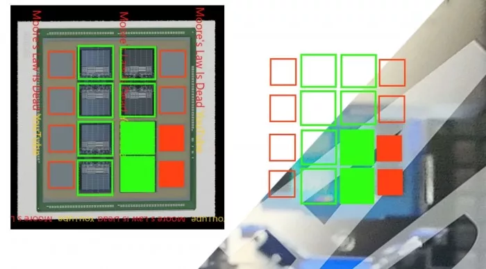
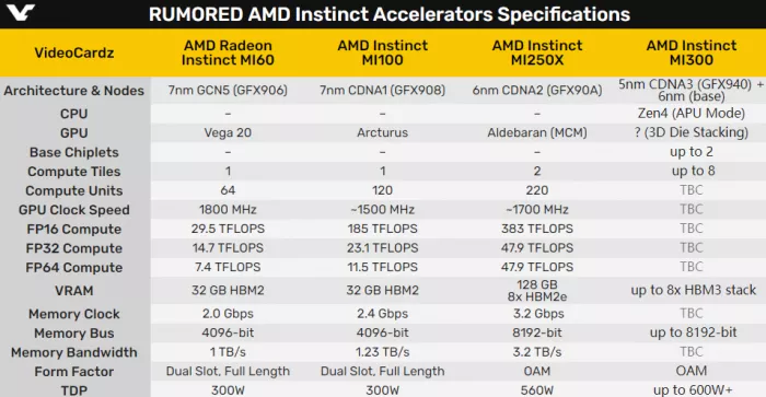
according to mlid , the internal design of mi300 is divided into three layers. At the bottom is a huge intermediate layer of 2750 square mm. In the middle is the base die (basic chip) of 6nm process, and then up is the compute die (Computing chip) and hbm3 memory chip of 5nm process.
The number and combination of various dies can be customized flexibly. The most common medium configuration is 2 6nm basic chips, 4 5nm computing chips and 4 hbm3, a total of 10.
The most high-end should be doubled. There are 4 basic chips, 8 computing chips and 8 hbm3, with a total of 20. The power consumption is expected to be about 600W, which is basically similar to the current top configuration.
In fact, as early as 2019, it was rumored that amd was planning "big APU" , which was expected to be called mi200 at that time, and now it seems that it will be realized on mi300.
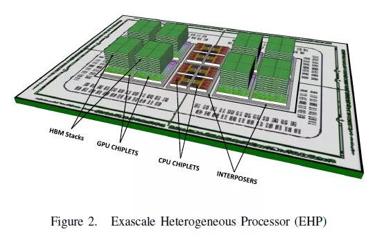
Another patent shows that AMD has designed a EHP (10 billion times heterogeneous processor) , which adopts multi chip integrated packaging, including CPU module, GPU module and HBM module , which is mi300?
AMD is really playing a big game!