Recently, at the future summit held in Antwerp, Belgium, IMEC (Microelectronics Research Center) released a report discussing the semiconductor process and technology roadmap until about 2036. IMEC is an authoritative semiconductor research institution established in 1984 and located in Europe. Its research interests include microelectronics, nanotechnology, information and communication system technology (ICT), chip process technology, component integration, nanotechnology, microsystem and components, packaging and other aspects.
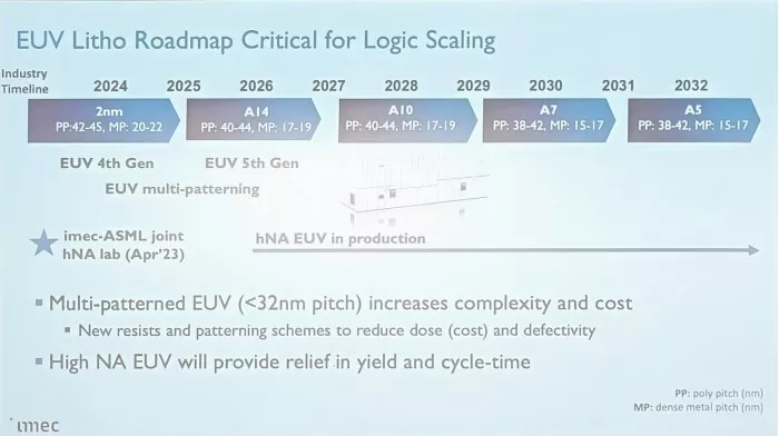
IMEC is not as famous as Intel, arm, ASML, TSMC, Samsung, SMIC and other chip designers and manufacturers, but it is also a heavyweight player, especially playing a vital role in basic technology research and industry standardization. IMEC has close cooperation with the above giants and is also cooperating with ASML to promote EUV lithography technology.
Before talking about the road map, first explain that the X nano process industry is labeled as "NX" (nanometer), and after nano, it will be "Amy" and labeled as "ax". In fact, Emmy is used after 2nm, and A14 is equal to 1.4nm.
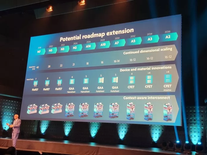
On the road map estimated by IMEC, each generation of process is stable and pushed forward at an interval of two years , but at present, it should be the initial production time rather than the commercial time of mass production, such as n33nm. The road map indicates 2022, but there is no actual product this year.
After that, N2, A14, A10, a7, A5, A3 and A2 will follow. The final A2 is 0.2nm, which is expected to be realized around 2036
Of course, the roadmap of different manufacturers is different. For example, Intel has an A18 and TSMC skipped N3.
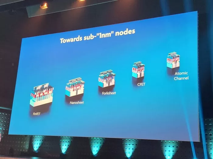
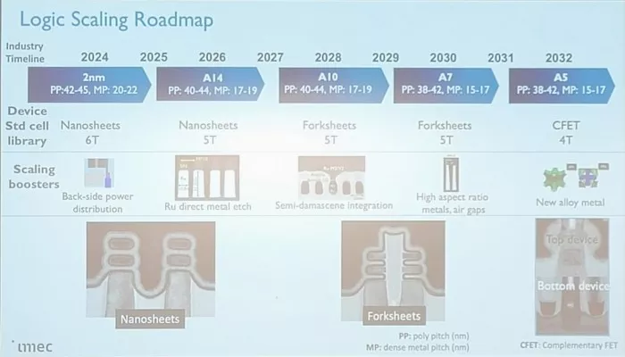
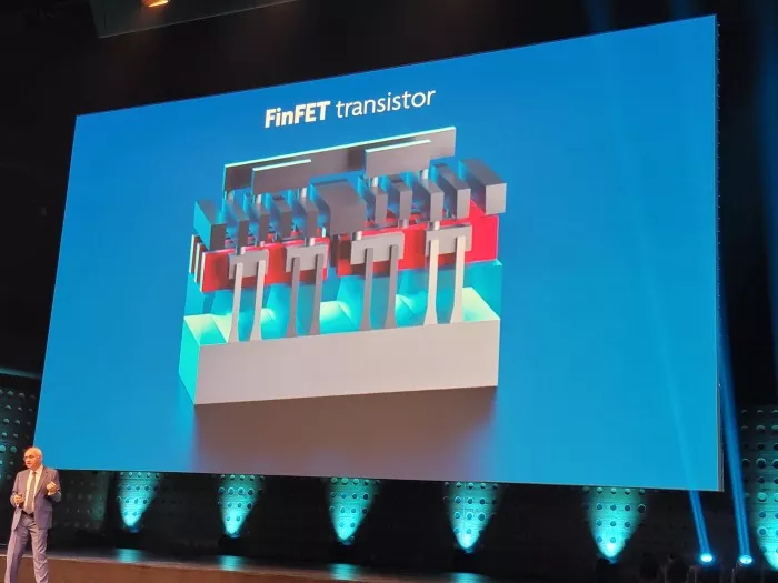
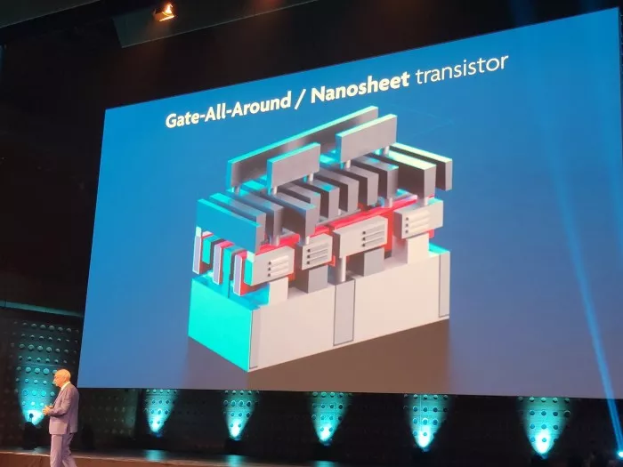
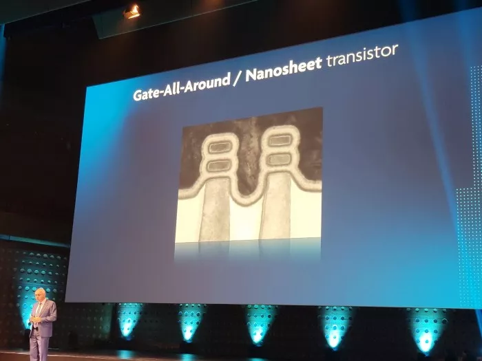
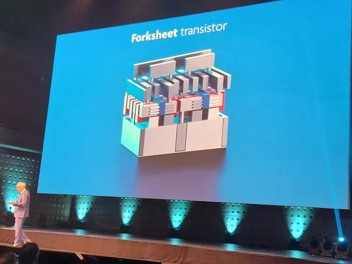
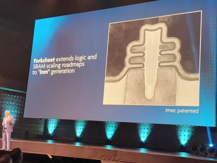
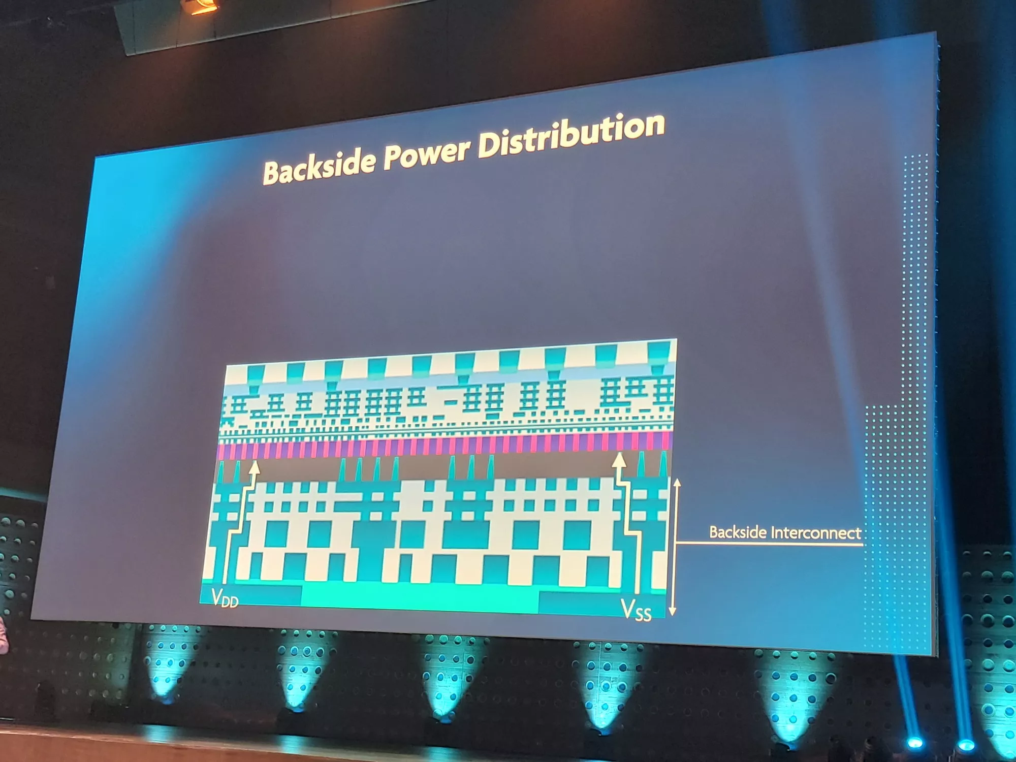
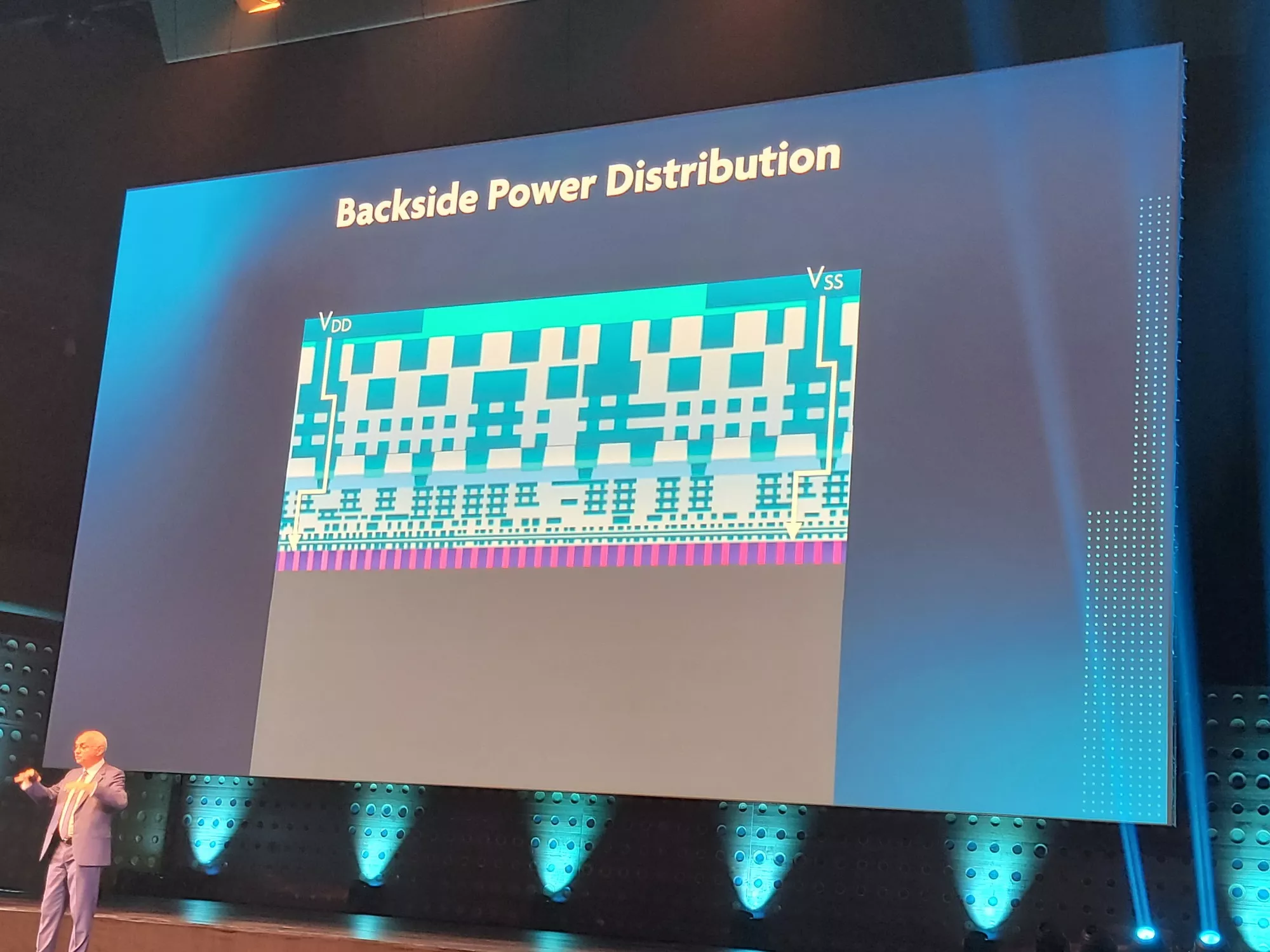
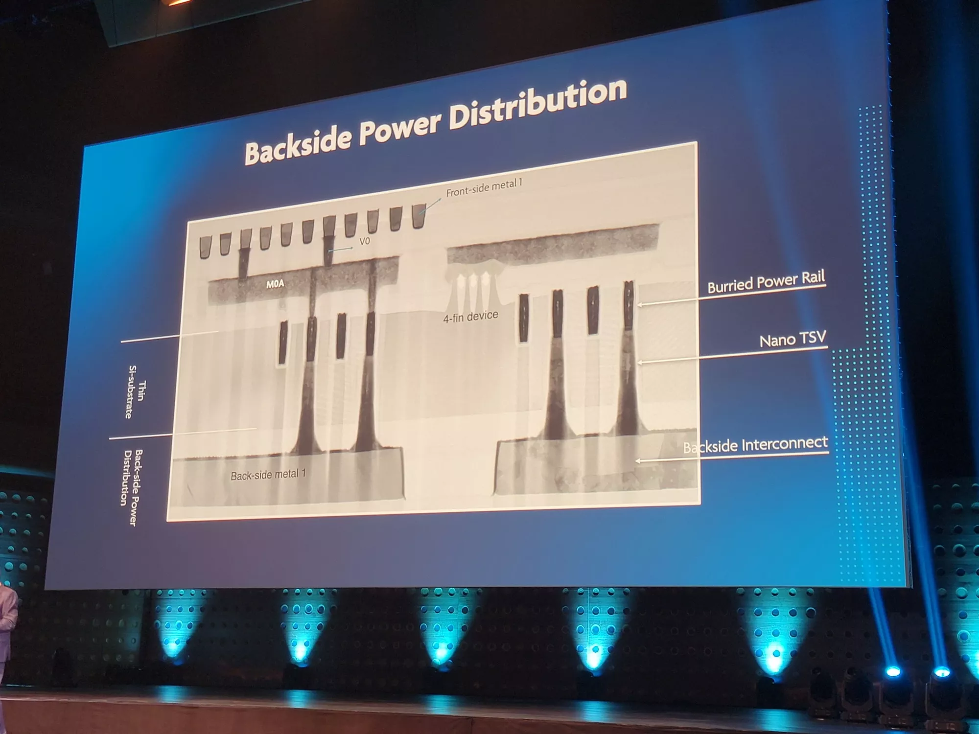
In terms of transistor technology, IMEC believes that the existing FinFET can only be maintained until N3 process, and then N2 and A14 will turn to GAA surround gate and nanosheet nano chip technology, while A10 and A7 will switch to forksheet**
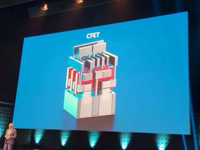
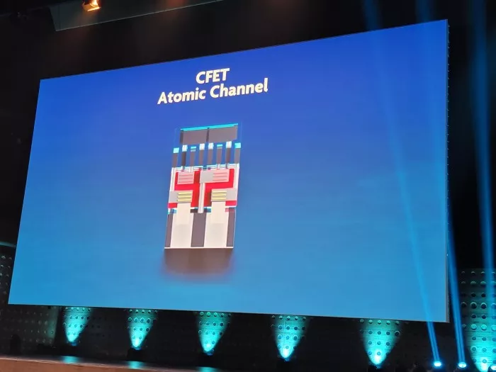
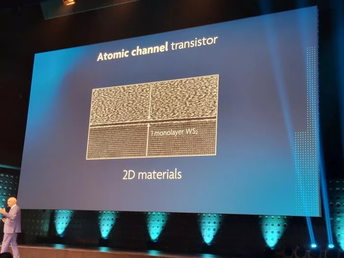
At the beginning of the A5 era, CFET complementary field effect transistors must be used, and in the A2 process, atomic atomic channels must be added
Naturally, each manufacturer's technical route is also different, and each process node has its own consideration of what technology to apply.
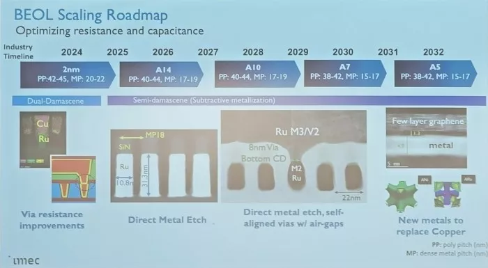
It is worth mentioning that it will be more difficult to further reduce the meta pitch, an important indicator to measure the progressiveness of the process. A10 process can reach 16nm, a7 process can only reach 16-14nm, and the subsequent A5, A3 and A2 processes will stay at 16-12nm.
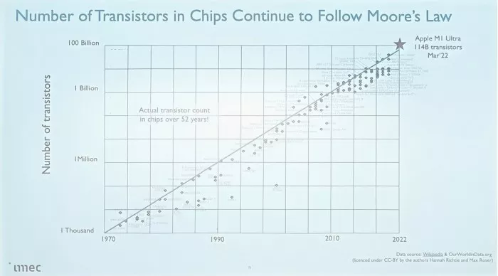
IMEC found that 52 years later, Moore's law is still strong in terms of the number of transistors, and the current king of the number of transistors belongs to Apple M1 ultra has reached 114 billion through dual core packaging.
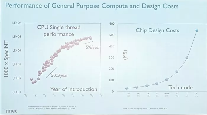
However , the cost of chip design is indeed soaring. The 16 / 14 nm process needs more than US $100 million, the 10 nm process is about US $180 million, the 7 nm process has soared to nearly US $300 million, and the 5 nm process is about US $550 million. It is sure to continue to soar in the future**