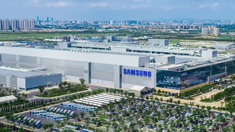
According To The Disclosure Of Foreign Media Quoted By Taiwan Media "Economic Daily" On May 2, Samsung Revealed In The Latest Briefing Released To Investors That Its 3nm Process Will Start Production In The Next Few Weeks, With A Faster Progress Than TSMC, Trying To Overtake In A Curve, And Officially Detonating The Fierce Competition Between TSMC And Samsung's Most Advanced Process This Year.
TSMC Has Never Commented On Its Competitors. TSMC Previously Pointed Out At The Law Conference That The 3nm With FinFET Architecture Will Be Mass Produced In The Second Half Of The Year According To The Original Plan, Which Will Be The "next Big Growth Node".
According To The Analysis Of Industry Insiders, Although Samsung Claims That 3nm Has Entered The Countdown Of Mass Production, From The Perspective Of Transistor Density And Efficiency, Samsung's 3nm Should Be The Same As 4nm Of TSMC's 5nm Family And Intel The Intel 4 Process Is Equivalent.
According To The Analysis Of Taiwan Media "Economic Daily", Samsung Named "3nm" As The Latest Process Progress, Which Has Won Face On The Surface, But It Still Lags Behind TSMC In Transistor Density And Efficiency, "in Fact, It Has Lost".
Techspot And Other Foreign Media Reported That Samsung Briefed Investors That It Is Fully Preparing To Make The 3nm Process Of GAA Architecture Enter The Production Stage In The First Half Of This Year, That Is, Start The Mass Production Process In The Next Eight Weeks, Which Means The Countdown Of 3nm Mass Production.
Samsung Said That Compared With The Current 7Nm FinFET Architecture Process, The Chips Produced By The New 3nm Process Can Work In A Low Voltage Environment Below 0.75 Volts, Reducing The Overall Power Consumption By 50%, Improving The Efficiency By 30% And Reducing The Chip Volume By 45%.
Analysts Point Out That The Power Leakage Process Of Samsung May Be 4 Nm Wider Than That Of Intel's Family Of Transistors, But The Performance May Be Better Than That Of Samsung's Family Of Transistors.
But The Biggest Variable We Can't Know At Present Is How Good Samsung's 3nm Process Yield Can Be. Samsung's Previous 4nm Process, Which Was Fully Developed, Resulted In A Significant Conversion Of Major Customers To Single TSMC Due To Its Low Yield. According To The Industry, Samsung's 3nm Yield Is Only About 10%, But It Has Not Been Confirmed By Samsung.
On The Other Hand, Samsung Did Not Disclose The Customers Using Its 3nm Process. In Contrast, Wei Zhejia, President Of TSMC, Previously Disclosed At The Legal Conference That Many Customers Participated In Its 3nm Application. It Is Expected That There Will Be More New Product Design Decisions In The First Year Compared With 5nm And 7Nm.
The Industry Believes That Apple、AMD And Yingji's)( ?site_id=242986&euid=&t=https://shouji.jd.com/ ) And Other Fields. TSMC Stressed That After The Mass Production Of 3nm In The Second Half Of This Year, It Will Take The Lead In PPA (efficiency, Power Consumption And Area) And Transistor Technology, And Has A Good Yield. It Is Confident That 3nm Will Continue To Win The Trust Of Customers.
In Addition, TSMC Has Also Embarked On A More Advanced 2nm Layout. It Is Expected To Conduct Risk Trial Production In 2024 And Mass Production In 2025. It Is Optimistic That 2nm Will Be The Most Advanced Technology In The Industry And The Most Suitable Technology To Support Customer Growth.

