Last month, Samsung foundry quietly announced that it was scheduled to start using 3gae technology to produce chips in the second quarter of 2022. As the first 3nm process technology in the industry to adopt GAA transistors, it can be seen that the term refers to "3nm", "ring gate transistor", and "early". However, to efficiently manufacture GAA transistors, wafer factories must also be equipped with new production tools The next generation of tools from applied materials will provide manufacturing support for GAA chips for wafer factories including Samsung
(from: Applied Materials official website,via AnandTech)
The new process is expected to achieve lower power consumption, higher performance and transistor density to meet the needs of chip designers. However, in recent years, this combination has been difficult to achieve - with the reduction of transistor size, wafer factories must overcome the negative effects such as leakage.
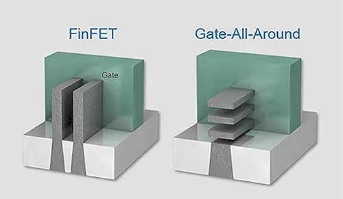
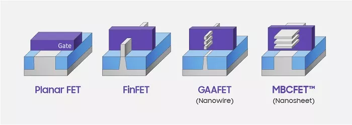
In order to maintain the performance and electrical parameters while scaling the transistor size, the chip industry has started the transition from planar transistor to FinFET (fin field effect transistor) in 2012 to increase the contact area between transistor channel and gate by making the gate higher.
Ten years later, as the distance between transistors gradually approaches the atomic level, its negative effects begin to appear more and more. Subject to this, the pace of FinFET process innovation is also slowing down.
Since Intel launched its FinFET technology based on 22nm more than a decade ago, chip manufacturers who plan ahead have been exploring how to turn to the next generation of ring gate technology.

As the name suggests, the channel of the ring gate field effect transistor (gaafet) is horizontal, and all four sides are surrounded by the gate, which solves the embarrassment related to leakage.
But this is not the only advantage of gaaget. For example, in gaafet based on nano chip / nano belt, the wafer factory can also adjust the channel width to obtain higher performance or reduce power consumption.
Samsung's 3gae and 3gap processes use the so-called nanobelt technology. The company even calls its gaafet multi bridge channel field effect transistor (mbcfet) to distinguish it from the nanowire competitive scheme.
Moreover, applied materials also claims that the GAA architecture reduces the variability of transistors. While other manufacturers are still discussing the advantages of gaafet over FinFET at various academic conferences, Samsung has taken the lead in deciding to transform to a new 4nm transistor process.
Samsung's current plan is to switch to new technology from 2022 to 2023, but there is also the possibility of ticket skipping in history. For example, the 3gae / 3gap node based on gaaft launched in 2019 was delayed until 2022 / 2023 respectively.
Last year, the Company re emphasized its plan to start 3gae production in 2022. But earlier, it said it would start mass production this quarter.
In addition to the courage of being the first to eat crabs, chip manufacturers always face arduous challenges. The products manufactured by Samsung based on 3gae node of mbcfet will inevitably encounter some risks.
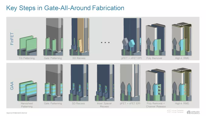
After all, manufacturers should not only reduce transistors to 3nm level, but also the manufacturing process of GAA is very different from FinFET.
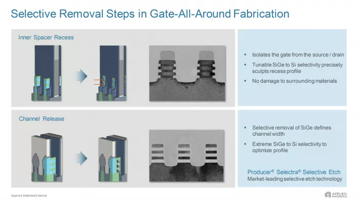
It is reported that the channel of GAA transistor needs photolithography, epitaxy, selective material removal and other molding processes. These processes enable chip manufacturers to fine tune channel width and uniformity for optimal performance / power consumption.
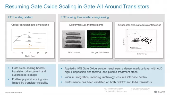
However, compared with FinFET, these epitaxial steps are much more complex, especially the deposition of multi-layer gate oxide and metal gate stack around the tiny 10 nm channel. Fortunately, the high vacuum integrated material solution (IMS) of applied materials can help.
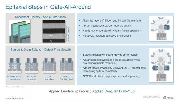
First, the company's producer selectra selective etch IMS tool removes unnecessary silicon germanium (SiGe) to isolate the gate from the source / drain and define the channel width without damaging the surrounding materials.
Secondly, the applied Centura prime EPI IMS tool can deposit ultra-thin gate oxide layers with the help of integrated atomic layer deposition (ALD), heat treatment, plasma treatment and metering steps.
Compared with the competitive solution, it can reduce the gate oxide thickness by 1.5 angstrom (atomic thickness unit). In this way, the thick gate can achieve higher driving current, so as to improve the performance of the transistor and increase the current leakage (a major disadvantage of the thin gate).
[background information]
Applied materials launched its first selectra etching system in 2016. So far, more than 1000 sets of chambers have been delivered to customers, so the industry is quite familiar with its use.
Although etching is a widely used process, its use and importance will further increase as the industry begins to shift to newer technologies, including processes based on GAA ring gate transistors.
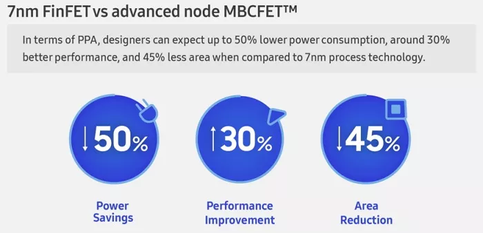
Taking Samsung 3gae process as an example, it is expected that its performance can be improved by 30% compared with 7llp, or the power consumption can be reduced by 50% / the area occupation can be reduced by 45%, which is enough to attract manufacturers to launch tough challenges to the new process in the short term.
At present, it is still quite difficult to use 3gae manufacturing technology relying on new transistor structure. In addition to the new electronic design automation (EDA) tools, Samsung also needs to invent new IP, adopt new design rules, and add new processes such as lithography, etching and deposition.
However, once a breakthrough is made, Samsung is expected to accumulate experience in the manufacturing and optimization of GAA transistors several years in advance of Intel and TSMC, so as to benefit more for a long time.
Moreover, the process can be used on hardware other than CPU. For example, Samsung DRAM can also benefit from smaller cell size / higher transistor density.