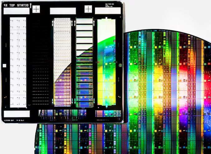
In order to successfully use EUV technology to produce chips, it took the semiconductor industry more than ten years to reach this stage However, according to the 2024-2025 roadmap recently updated by ASML in the Netherlands, it will take much less time to reach the next stage with high numerical aperture It is reported that the most advanced chips on the market have used the 5 / 4 nm manufacturing process.
(via AnandTech)
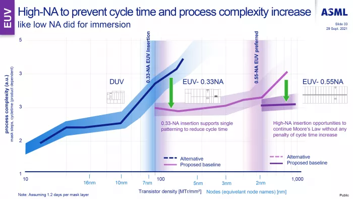
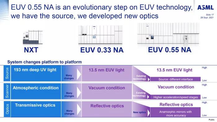
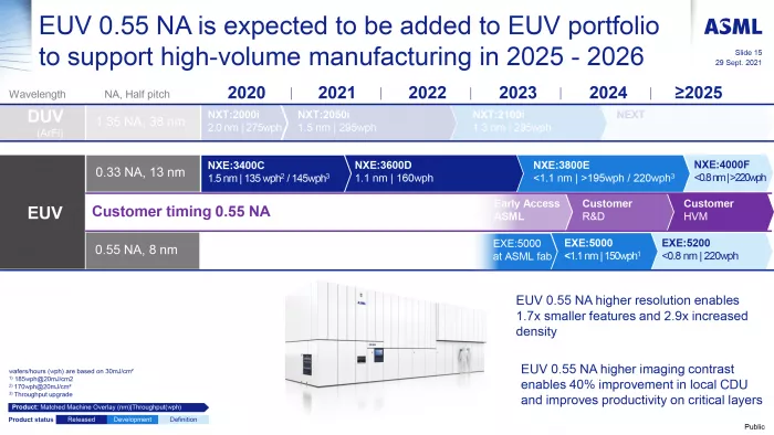
With ASML TWINSCAN nxe:3400c or similar system, combined with the optical flagship with 0.33 numerical aperture (NA), the machine can provide an accuracy of 13 nm.
This accuracy is sufficient for the process nodes of 7 / 6 nm (spacing 36~38 nm) and 5nm (spacing 30~32 nm) of the single-mode method.
As the semiconductor industry moves towards less than 5 nm (spacing < 30 nm), dual lithography exposure may be required in the next few years.
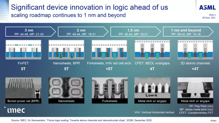
In the post 3nm node, ASML and its partners are developing a new EVU tool - TWINSCAN exe:5000 series, which has a 0.55 high NA lens, can achieve 8 nm accuracy, and is expected to eliminate the use of multiple exposures on more advanced process nodes.
New high NA scanners are still under development, and their structures are expected to be extremely complex, large and expensive - each costing more than $400million.
In addition to new optical devices, high numerical aperture also requires new light sources, and even a new wafer factory building to accommodate larger machines - all of which undoubtedly require a lot of additional investment.
Even so, after weighing the performance, power, area and cost (PPAC) of semiconductor devices, leading manufacturers of logic chips and storage devices are more willing to accept new technologies.
This means that high Na EVU scanners are crucial to the post-3 nm era, and the demand for high NA tools from various manufacturers will also be very strong.
A few weeks ago, ASML revealed that its TWINSCAN exe:5200 system with high numerical aperture (EUV 0.55 Na) received multiple orders from logic and DRAM customers in the first quarter of 2022.
In addition, Reuters reported last week that the company clarified in May that it would deliver high NA scanner orders for pilot use in 2024, and would deliver follow-up models with higher productivity (more than 5 orders) from 2025.
Interestingly, as early as 2020 - 2021, ASML said that it had received high NA purchase intentions from three major customers (undoubtedly Intel, Samsung and TSMC), and the total number reached 12 sets.
As for the first high NA system that ASML has begun to build, it will be completed in 2023 for IMEC and ASML customers to carry out relevant R & D work.
Peter wennink, ASML CEO, said: "we are making good progress in high NA EUV. At present, we have begun to integrate the first high NA system in the new clean room in Veldhoven.".
ASML received several exe:5200 system orders in the first quarter of this year, and received additional exe:5200 system orders in April.
Through these reservations, ASML received high NA system orders from customers of three logic chips and two storage manufacturers.
As the next generation high NA system of ASML, exe:5200 will greatly promote the improvement of lithography performance and productivity of the next generation.
It is reported that the TWINSCAN exe:5200 system of ASML is much more complex than the conventional TWINSCAN nxe:3400c machine, so the construction of original tools also takes longer time.
The company hopes to deliver up to 20 high NA systems in the medium term of the future, which may mean that its customers will have to fight for the priority of these machines.
Wennink added: "we are still in discussions with our supply chain partners to ensure that we can achieve the capacity of about 20 EUV 0.55 Na systems in the medium term.".
Up to now, only the Intel 18a process node has confirmed the use of ASML's high NA tool. The latter has disclosed that it will switch to mass production in 2025, which can roughly catch up with the time when ASML starts to deliver its high NA EUV system.
Recently, however, Intel postponed the starting time of 18a to the second half of 2024, and said that 18a manufacturing can be realized by using ASML TWINSCAN nxe:3600d or nxe:3800e system (probably by using multiple exposures).
Obviously, Intel hopes to accelerate the launch of its 18a process node to regain the leading position in process technology from TSMC.
However, for commercial chips, multiple exposure also means longer product cycle, lower yield, higher risk, and potentially lower capacity (even if there is still room for improvement).
Finally, leading semiconductor manufacturers, including Samsung, SK Hynix and micron, will inevitably adopt high NA EUV to mass produce chips. The problem is that they have not yet given an exact timetable.