Surging news learned from Peking University that on May 18, the research group of Professor Wang Xingjun of Peking University and Professor John E. Bowers of the University of California, Santa Barbara published the article "microcomb driven silicon optical systems" online in the journal Nature, which reported for the first time the new silicon-based optoelectronic on-chip integration system driven by the integrated microcavity optical comb in the world, indicating that the research team took three years to jointly tackle key problems, Finally overcome this worldwide problem.
According to the research team, optical comb, also known as optical frequency comb, has always been an important research hotspot in the international optical community because of its wide range of applications. Professor John Lewis Hall of National Institute of standards and technology and Professor Theodor h ä Nsch of Max Planck Institute of quantum optics in Germany won the 2005 Nobel Prize in physics for their outstanding contributions to optical combing.
In recent years, the chip level optical comb (micro cavity optical comb) has greatly expanded its application range because of its compact size and low cost. However, in most system level applications based on microcavity optical comb, only microcavity itself is an integrated device, and other components (including pump laser, passive / active processor and circuit control unit) are not integrated, which greatly weakens the advantages brought by microchip of microcavity optical comb in terms of cost, size and power consumption, The integration at the level of integrated optical comb system is of great significance to the practicability and popularization of optical frequency comb technology.
At the same time, in the past 20 years, silicon-based optoelectronic integrated chip technology (silicon light) with the help of mature CMOS (complementary metal oxide semiconductor) process can integrate the functional devices required by traditional optical systems on a large scale, greatly improve the speed and capacity of on-chip information transmission and processing, and bring revolutionary breakthroughs in the fields of next-generation data center, communication system, high-performance computing, automatic driving and so on. This is recognized as the core technology of the functional upgrading and industrial layout of modern information system, and it is the main position of competition in the field of Optoelectronics in the world.
At present, with the expansion of application market and the substantial improvement of system scale, the system architecture on silicon-based optoelectronic chip is evolving towards multi-channel and high parallel architecture, followed by the increasing demand for low-cost and high stability parallel light sources. However, due to the non luminescence of silicon materials, the realization of silicon-based lasers has always been a worldwide problem. The development of multi-channel parallel silicon-based light sources on silicon-based optoelectronic chips is recognized as one of the biggest bottlenecks in this field.
The research team led by Wang Xingjun provides the required light source brain for silicon-based optoelectronic integrated chip by directly pumping the integrated microcavity optical frequency comb by semiconductor laser. Combined with the mature and reliable integration solutions in the industry of silicon-based optoelectronic integration technology, it completes the efficient parallelization of large-scale integration system. Using this highly integrated system, T-bit rate micro communication and sub GHz microwave photonic signal processing are realized. A new architecture of high-density multi-dimensional multiplexing micro communication and micro processing chip level integration system is proposed, which creates the development of the next generation multi-dimensional silicon optical integration micro system sub discipline. Relevant research results are expected to be directly applied to data center, 5 / 6G communication, automatic driving, optical computing and other fields, providing a new research paradigm and development direction for the next generation on-chip optical electronic information system.
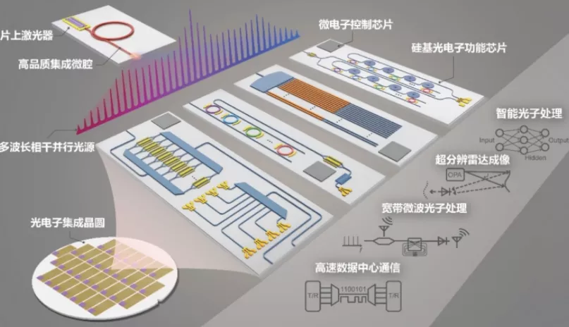
System diagram of silicon-based integrated optoelectronic chip driven by integrated microcavity optical comb. Peking University map
This work was completed by the State Key Laboratory of regional optical fiber communication network and new optical communication system, School of electronics, Peking University as the first unit. It is also an important achievement of the cooperation between Peking University and Pengcheng laboratory. It is one of the core contents of the major research tasks of the circuit and System Department of Pengcheng laboratory.