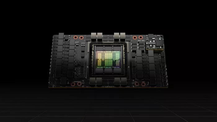
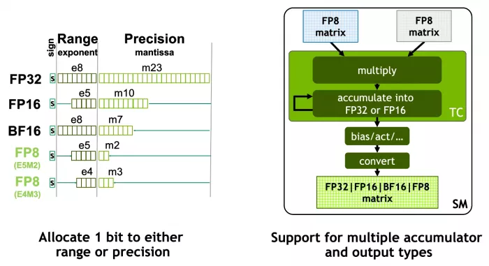
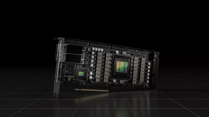
The paper specification of GH100 chip, which provides support for NVIDIA's next-generation H100 accelerator card, has surprised people. However, the white paper exposed over the weekend has given us a deeper understanding of it It is reported that Lvchang is actively using TSMC's N4 (4nm EUV) advanced technology to build hopper GPU, and the H100 chip is surrounded by six hbm3 high bandwidth video memory stacks.
(Figure via computerbase. De)
TechPowerUp It is pointed out that GH100 computing chip has 80 billion huge transistors, which is nearly 50% higher than ga100.
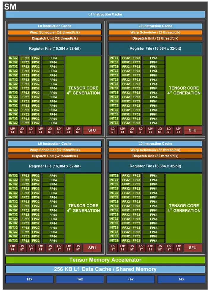
Design of stream processor for hopper GPU
Interestingly, with the support of 4nm EUV process, the chip area of GH100 is only 814 m2, which is smaller than ga100 (826 m2) manufactured based on 7Nm DUV (TSMC N7 process).
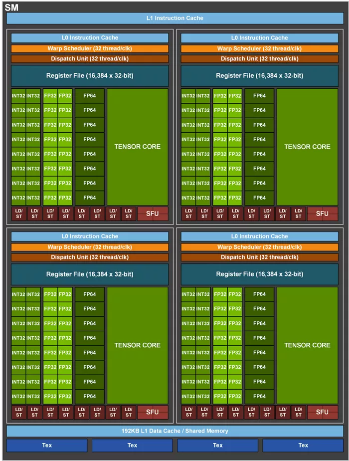
Design of stream processor for ampere GPU
It can be seen from the figure that the component hierarchy of NVIDIA GH100 is similar to that of the previous generation, and the main mathematical operation part is arranged on 144 groups of stream processors (SM).
GH100 has 18432 fp32 (single precision) / 9216 fp64 (double precision) CUDA cores, supplemented by 576 fourth generation tensor cores. In addition, one group of GPCS on silicon wafer has grating graphics units.
Given that GH100 has a 6144 bit hbm3 video memory bit width, NVIDIA may configure 80GB VRAM as standard, and the bandwidth is expected to exceed 3 TB / S (with ECC support).
The host interface has also ushered in a major upgrade, and the PCB with SXM shape is equipped with the latest generation nvlink interface (with 900 GB / s bandwidth).
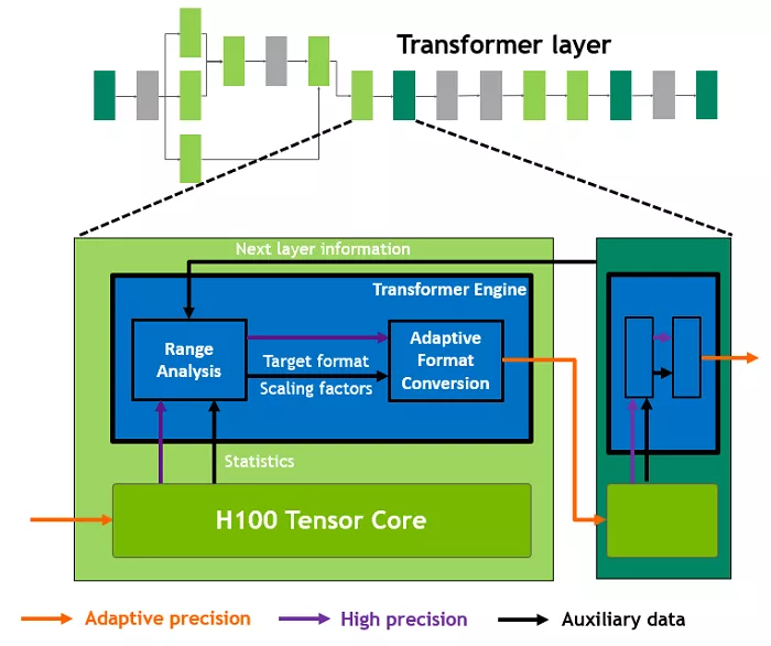
The AIC card version adopts PCIe 5.0 x16 (128 GB / s) interface, and both introduce the resource pooling function.
Finally, NVIDIA is squeezing more performance with higher power consumption - it can be seen that the typical power value of H100 is 700W, while that of A100 is only 400W.
However, H100 is not a full blood SKU. Even in the high-density SXM shape version, only 132 of 144 groups of SM units are enabled.
The PCIe card version only enables 114 SM units, and the maximum clock rate of both is 1.80 GHz.

